ASML to Ship Multiple High-NA Tools in 2025, Expands Production Capacities
by Anton Shilov on February 14, 2024 9:00 AM EST- Posted in
- Semiconductors
- Intel
- Samsung
- SK Hynix
- ASML
- TSMC
- Samsung Foundry
- High-NA
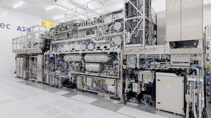
ASML began to ship its first High-NA lithography tool to Intel late last year ,and the machine will be fully assembled in Oregon in the coming months. Shipping only a single extreme ultraviolet (EUV) system with a 0.55 numerical aperture lens may not seem like too impressive, but the company aims to ship a much larger number of such devices this year, and further production increases in the coming years.
ASML did not disclose how many High-NA EUV litho tools it plans to ship this year, but the company has already announced that it had obtained orders for these machines from all leading makers of logic chips (Intel, Samsung Foundry, TSMC) and memory (Micron, Samsung, SK Hynix), and that the total number currently stands between 10 and 20 systems. Essentially, this means that High-NA EUV will be widely used. But the question is when.
ASML's High-NA EUV Twinscan EXE lithography systems are the company's next-generation flagship production tools that will enable chipmakers to decrease critical dimensions of chips to 8nm in a single exposure, a substantial improvement over 13nm offered by today's Low-NA EUV Twinscan NXE. But that improvement comes at a cost. Each Twinscan EXE costs €350 million ($380 million), which is over two times more than the price of a Twinscan NXE (€170 million, $183 million).
The steep price tag of the new tools has led to debates on its immediate economic feasibility as it is still possible to print 8nm features using Low-NA tools, albeit using double patterning, which is a more expensive and yield-impacting technique. For example, Intel is expected to insert High-NA EUV lithography into its production flow for its post-18A fabrication process (1.8 nm-class) sometimes in 2026 – 2027, whereas analysts from China Renaissance believe that TSMC only intends to start using these tools for its 1 nm-class production node sometime in 2030. Other industry analysts, like Jeff Koch from Semianalysis, also believe that the broader adoption of these high-cost machines might not occur until it becomes economically sensible, anticipated around 2030-2031.
Nevertheless, ASML executives, including chief executive Peter Wennink, argue that elimination of double patterning by High-NA EUV machines will provide enough advantages — such as process simplification and potentially shorter production cycle — to deploy them sooner than analysts predict, around 2026-2027.
Having secured between 10 and 20 orders for the High NA EUV machines, ASML is preparing to increase its production capacity to meet the demand for 20 units annually by 2028. That said, the uncertainties around other chipmakers' plans to use High-NA tools in the next two or three years raises concerns about potential overcapacity in the near term as ASML ramps up production.


8 Comments
View All Comments
nicolaim - Wednesday, February 14, 2024 - link
I don't think the proofreader made it to the end..."Meanwhile, uncertainties about plance of chipmaker"
Threska - Wednesday, February 14, 2024 - link
A plance shortage.Ryan Smith - Wednesday, February 14, 2024 - link
Thanks!bob27 - Monday, February 19, 2024 - link
Now it says "chipmarkers"Threska - Wednesday, February 14, 2024 - link
Important takeaway is expensive tools and process means more expensive chips. So remember that next time we're complaining about GPU prices.FunBunny2 - Thursday, February 15, 2024 - link
ah, the Capitalist's dilemma: automate further/better/cheaper (on a per-widget basis) is profitable only if excess output from further/better/cheaper can be shifted at a nice price. mostly, so far, it's resulted in consolidation of function from what-used-to-be multiple chips into ginormous monoliths. the GPU situation is a bit different, in that it always benefits from further/better/cheaper just because what it does is just brute-force computing.now that bitcoin is at/near the next having (only ~1.5 million coin remain to be mined) that lode is about shot.
will AI suck up the new-found largesse? only The Shadow knows. hallucination be damned.
FullmetalTitan - Saturday, February 17, 2024 - link
High-NA tools won't be used for GPU die anytime soon. The increase in feature fidelity comes at a cost of maximum shot area, so a single exposure drops from 858mm^2 (26x33mm) to 429mm^2 (26x16.5mm).That is a necessity of the new optics required for high NA machines, they use anamorphic lenses to compensate for changes to the light path that would otherwise lead to interference effects that degrade image quality. The new lenses stretch the mask pattern in only one direction, so the printable area per shot is halved in that direction.
Eventually designers can work around this with mask stitching, but that would still require 2 exposures and masks, both of which are pretty expensive.
Most likely we will see GPU designs land at 3/4/5nm design nodes and stay there for a couple generations, but this has historically been when the best and most innovative changes to designs come about.
Zoolook - Sunday, February 25, 2024 - link
There is a reason both Intel and AMD have been working on gpu chiplets, Nvidia seems to be trying to catch up with their next designDon't worry, gpus will not be stuck on older process nodes at lest not due to shrinking aperture size, more likely cost of new nodes compared to old will keep to be the arbiter of progress.