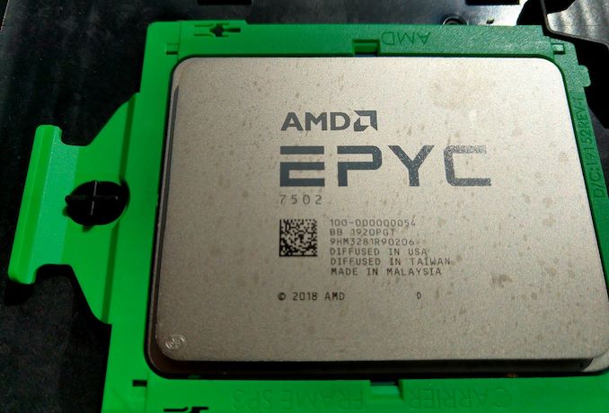
AMD May Be Prepping More 280 W EPYC Enterprise CPUs
by Anton Shilov on October 21, 2019 4:00 PM EST
Back in September, AMD announced its 64-core EPYC 7H12 processor - a 280 W TDP behemoth with an increased base frequency designed specifically for the high-performance computing market. Based on AMD’s Product Master list inadvertently published by the company earlier this week, the company may release more EPYC CPUs with an extended TDP.
As it turns out, the EPYC 7H12 will not be the only Rome CPU with a 280 W TDP. AMD’s Product Master document lists the EPYC 7R22 and the EPYC 7R32 with a 280 W TDP, as well as the EPYC 7V12 with a 240 W TDP. We have no idea whether these CPUs are to be released for the wider market, are for OEMs only, or if they are in the plans, or which market segments they will address. Meanwhile, a high TDP might indicate that AMD intends to release more processors for HPC in general or maybe even a specific HPC customer, or they might have a specific feature not available on other processors.

From AMD's Master Product Document
The document also mentions various EPYC CPUs with TDP levels of 180 W or 225 W, but nothing else is known about these processors.
AMD’s 64-core EPYC 7H12 with a 256 MB L3 cache features a 2.60 GHz base frequency, a 3.30 GHz turbo frequency, as well as a 280 W TDP. Compared to the EPYC 7742, the 7H12 has a 350 MHz higher base clock, a 100 MHz lower turbo clock, but a 55 W higher TDP. While the CPU is socket compatible with other Rome processors and support the same features, it is expected to be used primarily in large HPC datacenters that need a maximum sustained performance and that do not care about power consumption.
| AMD EPYC 7002 Processors (2P) | ||||||
| Cores Threads |
Frequency (GHz) | L3* | TDP | Price | ||
| Base | Max | |||||
| EPYC 7H12 | 64 / 128 | 2.60 | 3.30 | 256 MB | 280 W | ? |
| EPYC 7742 | 64 / 128 | 2.25 | 3.40 | 256 MB | 225 W | $6950 |
| EPYC 7702 | 64 / 128 | 2.00 | 3.35 | 256 MB | 200 W | $6450 |
| EPYC 7642 | 48 / 96 | 2.30 | 3.20 | 256 MB | 225 W | $4775 |
| EPYC 7552 | 48 / 96 | 2.20 | 3.30 | 192 MB | 200 W | $4025 |
There is one important thing to note about AMD’s Product Master list, which is an internal document that contains OPN codes along with US ECCN, HTS, and CCATS codes that are required by the US export regulators. The paper lists hundreds of products, yet some of them are potential products that may or may not be released, whereas other are off-roadmap client-specific SKUs not supposed to be generally available.
Related Reading
- AMD’s New 280W 64-Core Rome CPU: The EPYC 7H12
- AMD Rome Second Generation EPYC Review: 2x 64-core Benchmarked
- The AMD 2nd Gen EPYC "Rome" Launch Live Blog
- AMD Zen 2 Microarchitecture Analysis: Ryzen 3000 and EPYC Rome
Sources: AMD, Reddit, Komachi_Ensaka/Twitter, Planet3DNow.de


22 Comments
View All Comments
gchernis - Monday, October 21, 2019 - link
256 GB L3. Nice!Valantar - Monday, October 21, 2019 - link
I wonder how big that die would need to be.Samus - Monday, October 21, 2019 - link
Literally the entire wafer :)deil - Tuesday, October 22, 2019 - link
nah, we already have 1G in 10x20 mm so propably like 2 rome CPU's for l3 alone. not that muchshabby - Monday, October 21, 2019 - link
The race to 1 gigabyte of l3 cache is on! 😁Kevin G - Tuesday, October 22, 2019 - link
Depending on how you define that, the Xeon Phi did that with its MCM. It didn't save on latency much it had much higher bandwidth than the six channel DDR4 bus it was socketed in. It would have been interesting to have had a third generation of Xeon Phi with larger HBM2 stacks. Shame Intel's 10 nm troubles killed off the part early on.Gondalf - Tuesday, October 22, 2019 - link
Xeon Phi was not killed for 10nm troubles but because there is a GPU for server at the horizon (on 10nm)Kevin G - Tuesday, October 22, 2019 - link
Check the time line. It was killed for lack of 10 nm availability. It was to be Intel's first big die on 10 nm with a release date of . Intel formally killed off Knight's Hill in 2017 which was the same year it was initially due. That wasn't supposed to be the first 10 nm chip either. Cannon Lake was originally due in late 2015/early 2016. With 10 nm slipping, Intel had nothing to compete with nVidia in the HPC space during this time. It made no sense to bring a relatively low volume product to market that would not be able to compete.Intel's Xe line up is indeed replacing Xeon Phi but that was only set in stone after they already had killed off Knight's Hill.
FullmetalTitan - Thursday, October 24, 2019 - link
According to one of the project managers at Intel during that time frame, that line of processors was already on precarious ground. Its continuance was predicated on a smooth 10nm development, which clearly didn't happen. Technically speaking, 10nm failures killed the product line, but more accurately phrased, 10nm failings just kicked out the last supporting post for the project.nandnandnand - Tuesday, October 22, 2019 - link
1-4 GB of L4 cache stacked on the Zen 4 I/O die. Hopefully on every part from mobile to server.