Semiconductors
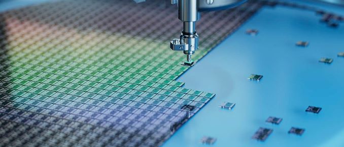
One of the core challenges that Rapidus will face when it kicks off volume production of chips on its 2nm-class process technology in 2027 is lining up customers. With Intel, Samsung, and TSMC all slated to offer their own 2nm-class nodes by that time, Rapidus will need some kind of advantage to attract customers away from its more established rivals. To that end, the company thinks they've found their edge: fully automated packaging that will allow for shorter chip lead times than manned packaging operations. In an interview with Nikkei, Rapidus' president, Atsuyoshi Koike, outlined the company's vision to use advanced packaging as a competitive edge for the new fab. The Hokkaido facility, which is currently under construction and is expecting to begin equipment installation...
AMD Amends Wafer Supply Agreement with GlobalFoundries: 7nm Freed, 12nm+ Targets Set Through 2021
AMD on Tuesday said it had amended its wafer supply agreement with GlobalFoundries. Under the terms of the new deal, the two companies agreed about prices and volumes of...
37 by Anton Shilov on 1/29/2019
Intel Considers $11 Billion Fab in Israel
Late last year Intel announced massive plans to increase its global chip production capacities by upgrading, expanding, and equipping four of its fabs. As it turns out, the company...
37 by Anton Shilov on 1/29/2019
TSMC Chip Yields Hit By Bad Chemical Batch
TSMC on Monday said that some of the wafers it has processed recently have lower yields because of a chemical it uses during production. The company began investigation and...
28 by Anton Shilov on 1/29/2019
ASML to Ship 30 EUV Scanners in 2019: Faster EUV Tools Coming
ASML said last week that it planned to ship 30 extreme ultraviolet scanners in 2019, up significantly from 2018. The plan is not surprising, as demand for EUV lithography...
17 by Anton Shilov on 1/28/2019
ASML, Carl Zeiss, and Nikon to Settle Legal Disputes Over Immersion Lithography
Embroiled for some time now in legal disputes concerning immersion lithography, ASML, Carl Zeiss, and Nikon, this week signed a memorandum of understanding relating to a plan to once...
10 by Anton Shilov on 1/25/2019
TSMC: 7nm Now Biggest Share of Revenue
As process node technology gets ever more complex, it costs big dollars to develop and then building chips on the process is also a very costly process. The big...
44 by Ian Cutress on 1/17/2019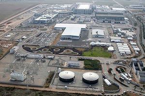
Israeli Parliament Approves Intel Fab 28 Expansion Grant
The Finance Committee in Israeli parliament this week approved a grant to Intel to expand its Fab 28 production facility in Kiryat Gat. The decision confirms that Intel’s expansion...
24 by Anton Shilov on 12/28/2018
IBM to use Samsung 7nm EUV for Next-Gen POWER and z CPUs
IBM has announced it has signed an agreement with Samsung Foundry to produce its next-generation processors. This includes processors for IBM Power Systems, IBM z, and LinuxONE systems, all...
24 by Anton Shilov on 12/21/2018
Intel to Expand Production Capacities at Multiple Fabs
Intel this week reiterated plans to expand its production capacities in a bid to more quickly respond to increased demand. In the coming years the company intends to increase...
24 by Anton Shilov on 12/19/2018
Intel Further Boosts CapEx to Meet Demand for 14nm Chips
Earlier this year Intel said that it had reaffirmed its plan to invest $1 billion in a bid to increase the number of chips made using its 14 nm...
21 by Anton Shilov on 12/6/2018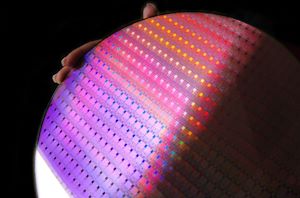
Intel: EUV-Enabled 7nm Process Tech is on Track
Originally planned to enter mass production in the second half of 2016, Intel’s 10 nm process technology is still barely used by the company today. Currently the process is...
79 by Anton Shilov on 12/6/2018
GlobalFoundries and Chinese Authorities Reconsider Plans
Because of its renewed focus on specialized process technologies and competition, GlobalFoundries has opted to reconsider its plans concerning its Fab 11 located near Chengdu, China. Rather than offer...
21 by Anton Shilov on 11/26/2018
GlobalFoundries Establishes Avera Semiconductor: a Custom Chip Company
GlobalFoundries this week announced that it has spun off its ASIC Solutions division, establishing Avera Semiconductor, a wholly owned subsidiary that will help fabless chip developers to design their...
11 by Anton Shilov on 11/2/2018
Samsung Starts Mass Production of Chips Using Its 7nm EUV Process Tech
Samsung Foundry on Wednesday said that it had started production of chips using its 7LPP manufacturing technology that uses extreme ultraviolet lithography (EUVL) for select layers. The new fabrication...
42 by Billy Tallis & Anton Shilov on 10/17/2018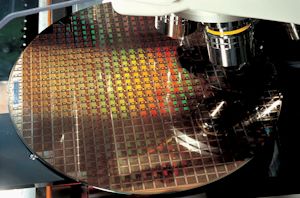
TSMC: First 7nm EUV Chips Taped Out, 5nm Risk Production in Q2 2019
Last week, TSMC made two important announcements concerning its progress with extreme ultraviolet lithography (EUVL). First up, the company has successfully taped out its first customer chip using its...
50 by Anton Shilov on 10/9/2018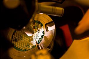
GlobalFoundries Enables Connectivity IP: New RF SOI and Ensigma BLE on 22FDX
GlobalFoundries this week made two important announcements concerning its radio and connectivity-related capabilities. First up, the company said that Imagination’s Ensigma connectivity IP is now available for its 22FDX...
2 by Anton Shilov on 9/27/2018
Cadence Announces The Tensilica DNA 100 IP: Bigger Artificial Intelligence
Cadence is an industry player we don’t mention nearly enough as much as we should - they make a lot of IP and specialises in accelerator blocks which augment...
9 by Andrei Frumusanu on 9/19/2018
Samsung Foundry Updates: 8LPU Added, EUVL on Track for HVM in 2019
Samsung recently hosted its Samsung Foundry Forum 2018 in Japan, where it made several significant foundry announcements. Besides reiterating plans to start high-volume manufacturing (HVM) using extreme ultraviolet lithography...
29 by Anton Shilov on 9/6/2018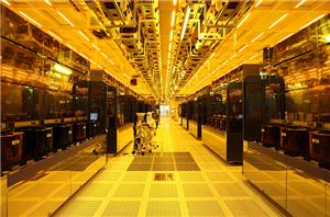
Micron to Expand Its Fab 6 in Virginia, Build New R&D Center
Micron this week announced plans to expand production of DRAM and NAND memory at its fab in Manassas, Virginia. In total, Micron intends to invest $3 billion into the...
11 by Anton Shilov on 8/31/2018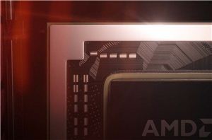
AMD's 7nm CPUs & GPUs To Be Fabbed by TSMC, on Track for 2018 - 2019
With the announcement that its long-time manufacturing partner (and outright former fab) GlobalFoundries is dropping out of the race for bleeding-edge manufacturing nodes, the second big question of the...
28 by Ryan Smith & Anton Shilov on 8/27/2018


